Fehlersuche 16kb-SRAM Karte SKS KISS 2116

    • Offizieller Beitrag

    Hallo!


    Wie bereits geschrieben, erkennt meine KISS nach dem Tausch des CRT 5027 ICs von einer P2 Karte die 16kB SRAM Karte nicht mehr.

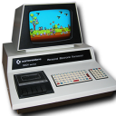
    Ohne SRAM Karte (MC80 1010E 12 811 187, 80-10-5, K18.00.330-E) läuft sie, siehe auch : About TMS9927/5027 internals


    Wahrscheinlich hat das eine mit dem anderen nichts zu tun. Wie auch immer, die Vermutung liegt nahe, daß der Fehler auf der SRam Karte zu suchen ist.


    Jetzt habe ich mir die Karte heute einmal angesehen und begonnen, die ICs auszulöten und in slabbi s genialem Speichertester zu prüfen.


    Bisher habe ich sieben (7 !!! ) defekte 2114 1024kx4 SRAM gefunden.


    Das könnte erklären, daß die von helwie44 † freundlicherweise zur Verfügung gestellte SKS Systembibliothek Inbetriebnahme SKS KISS II 2116 nicht funktioniert, weil der Speicher teildefekt war?


    Weiterhin habe ich 2 Tantalen gefunden mit > 30 Ohm ESR.


    Soll ich wieder Tantal-Kondensatoren einlöten, oder tun es auch Elkos mit gleicher Kapazität? Dieser Thread hier deutet darauf hin, daß man das durchaus machen kann https://www.mikrocontroller.net/topic/169958 Normale Elkos explodieren wenigstens nicht.

  • Das sind ganz schön viele. Wie viele RAMs waren es denn insgesamt?


    Anstelle der Tantal-Elkos kannst du auch andere Elkos nehmen. Tantal-Elkos haben nur einen niedrigeren ESR und eine etwas höhere Lebensdauer, da diese nicht eintrocknen. Um ein wenig die Spannungsversorgung zu stützen, reichen "normale" Elkos aus und 8000+h Lebensdauer sollten doch reichen *g* Die Tantal-Elkos hat man früher auch gerne deshalb genommen, weil sie sehr klein sind. Vergleiche aber einmal einen 1000uF/25V von 1980 mit einem von heute. Die Elkos sind insgesamt ziemlich geschrumpft.

    Erklärung gem. "§ 6 Übertragung von Nutzungsrechten" Abs. (1) der Nutzungsbedingungen:

    Hiermit erkläre ich, dass alle meine Postings mit deren Inhalten nicht der Creative Commons License (CC BY-NC-SA) unterliegen. Ich räume diesem Forum jedoch für meine eigenen Inhalte deren Veröffentlichung bis auf Widerruf ein.

  • Das sind ganz schön viele. Wie viele RAMs waren es denn insgesamt?

    kommt mir auch krass viel vor. 32 Stück sind insgesamt auf der Platine.

    Oder glaubst Du, daß vielleicht der Test zu "konservativ" ist?

    Bei SRAMs sind die Timings nicht kritisch, wenn da ein Test fehlschlägt, dann ist der Chip zu 99.99% hinüber.

    Ich hatte bei 6550 knapp 50% fehlerhafte. Hatte ich auch erst nicht dran geglaubt und diese einzeln im PET geprüft. Waren tatsächlich alle defekt.

    Erklärung gem. "§ 6 Übertragung von Nutzungsrechten" Abs. (1) der Nutzungsbedingungen:

    Hiermit erkläre ich, dass alle meine Postings mit deren Inhalten nicht der Creative Commons License (CC BY-NC-SA) unterliegen. Ich räume diesem Forum jedoch für meine eigenen Inhalte deren Veröffentlichung bis auf Widerruf ein.

    • Offizieller Beitrag

    So, nun ist die Platine fast nackt.

    Die Logik ICs waren alle ok.

    Die Bustreiber kann ich nicht testen.

    Nun kann ich Sockel einlöten und die RAM Karte wieder bestücken.

    Wusste gar nicht, daß Tantal Kondensatoren auch im ESR degradieren können. Dachte immer, daß sei Alu-Becherelkos vorbehalten

    Weiß jemand, wo man die axialen 100nF Kunststoff-Folienkondensatoren herbekommt? Einer der beiden ist defekt ("open circuit or low capacitance", der andere zeigt seine 100nF)

  • I checked Mouser and the capacitors you need seem to be in production.


    I know that's uncalled but... I don't remember having seen the schematics for this module. Now that your board is mostly unpopulated it could be a good time to document its logic.


    About soldering them again, my advice is to solder sockets in their place. It wouldn't look as pretty as before but service and check would be easier and faster.


    Regards,

    Jaume

    When I tried to list all retro systems I have at home, the "The message is too long, must be under 500 characters" error appears! :lol:

    • Offizieller Beitrag

    I know that's uncalled but... I don't remember having seen the schematics for this module. Now that your board is mostly unpopulated it could be a good time to document its logic.

    Yes, using sockets is already my plan,

    Do you have a good idea of the workflow to document the PCB?

    I have no experience using PCB Layout software (up to now, at least).

  • Nur ein Tipp: Tantals wurden bzw. werden gerne zur Stützung der Betriebsspannungen eingesetzt, eben wegen sehr

    niedrigem ESR, kleiner Baugröße und dem "nicht Austrocknen".


    Das geht gut, solange die Betriebsspannungen nicht schlagartig eingeschaltet werden. Was daher gar nicht gut ist, wenn das Netzteil bereits Spannung hat und das Einschalten der Elektronik über einen Schalter auf der Niederspannungsebene stattfindet. Der dann wegen des niedrigen ESR fliessende Ladestrom kann dann extrem hoch sein.


    Ich weiss natürlich nicht, ob das bei den betrachteten Rechnern so möglich ist. Aufpassen, wenn zu Testzwecken Labornetzteile eingesetzt werden und das Einschalten durch Stecken eines Kabels ins Netzteil erfolgt!


    Verpolung oder auch noch so kurze Überspannung kann einen Tantal Kondensator unrettbar beschädigen, während ein Elko sich davon normalerweise wieder erholt.

  • Ich würde da nicht so viel Aufhebens machen, ob man nun auf eine 30-40 Jahre alte Platine einen Tantal-Elko oder Aluminium-Elko einsetzt.

    Die heutigen Elkos sind im Längen besser als die Tantals, die man damals verbaut hat.

    Selbst ohne Elkos wir die Platine vermutlich anstandslos laufen. Möchte man die Spannung etwas gestützt haben, reicht ein einigermaßen passender Elko, dabei ist die Kapazität auch eher zweitrangig (die hatten früher teilweise -50%/+100% Abweichung).


    Auch die Stützkondensatoren bzw. Abblockkondensatoren an den ICs sind bei den alten Schaltungen eher unkritisch. Nach Daumenregel ist alles zwischen 10-100nF ok. Bei heutigen Schaltungen sind 100nF eher nicht mehr zeitgemäß, aber bei einer alten Platine ist das ziemlich egal.


    Guckt euch einmal eine über 40 Jahre alte Platine vom PET unter Oszilloskop an. Selbst mit den gealterten Komponenten und den teilweisen katastrophalen Signalen läuft das Teil. Da ist der Unterschied Tatal-Elko oder Aluminium-Elko bei einer Reparatur nun wirklich vernachlässigbar. Ich würde den Tantal nur aus einem Grund bevorzugen und das wäre die Optik. ;)


    Obiges heißt nicht, dass man jetzt Kondensatoren wahllos wählen könnte, es gibt schon Einsatzzwecke, da sollten diese korrekt ersetzt werden. Aber es kommt halt auf den Einsatzzweck an.


    Zu dem Thema findet man hier einiges:

    http://www.dse-faq.elektronik-…ium.de/dse-faq.htm#F.14.1

    Erklärung gem. "§ 6 Übertragung von Nutzungsrechten" Abs. (1) der Nutzungsbedingungen:

    Hiermit erkläre ich, dass alle meine Postings mit deren Inhalten nicht der Creative Commons License (CC BY-NC-SA) unterliegen. Ich räume diesem Forum jedoch für meine eigenen Inhalte deren Veröffentlichung bis auf Widerruf ein.

  • Do you have a good idea of the workflow to document the PCB?

    I have no experience using PCB Layout software (up to now, at least).

    The first step is disassembly, which has been already done. Boards without components (like backplanes) don't need this first step. If there is any patch involving wires has to be annotated before their disassembly. Next, a drawing of the board has to be made and the references of the components annotated in it. The next step is to find the pinouts of the components. You may find them in their datasheet, for the connector you may find its pinout at helwie44 † 's website. I imagine in this case column C would not be used, if that's the case then there's less work to do. Once the pinouts are known, the layout may be recorded using the most advanced technology available: paper and pencil. Lot of work can be avoided with the memories: they are likely to have shared data and address bus... but being 2114 there are two 4 bit data busses (the 8 bit one is split in two halves). After this, the logic: who sends and who receives, and that's all. For the generation of schematics, I use Kicad. It's very user-friendly and allow to create new symbols and footprints which is ideal for the long-obsolete 2114 which is not in the libraries. If you use it, I could either provide my custom library or directly creating the schematics from your drawings.


    This information is important, not only during repairs but also for diagnostics. If we knew what ic contains a particular memory cell, it could be discovered by software and by then, the work of having the 96 memory chips desoldered would be history.


    Regards,

    Jaume

    When I tried to list all retro systems I have at home, the "The message is too long, must be under 500 characters" error appears! :lol:

  • jlopez : Shall I remove the remaining parts and Scan the board form both sides?

    In this case it is not necessary. This board is simple.

    When I tried to list all retro systems I have at home, the "The message is too long, must be under 500 characters" error appears! :lol:

  • Too late.:sense::sense:I had to kill the 96pin DIN connector because ist was crimped and glued to the board ...


    As you can see, some of the middle row pins are used.

    Of course, middle column is B and it carries control signals like -MemR and -MemW.


    You could try to recover the stickers on the connector using a hairdryer. If you succeed they could be glued on the new part.


    It's not necessary for you to continue with the documentation, if you are busy. If you could provide the ic references and their positions, I could do it while you reassemble the board.


    I didn't want you to remove the connector but as you have done it, I must thank you. I'm trying to remove it from the CPU module and thought it was stuck... if you say it is glued and I have to kill it anyways it would save both time and damage.


    Regards,

    Jaume

    When I tried to list all retro systems I have at home, the "The message is too long, must be under 500 characters" error appears! :lol:

    • Offizieller Beitrag

    Wow, well done!


    I would still scan it. It could simplify the reproduction of the board.

    Just my two cents...

    Scan already attached in #18 - or do you mean something different?

    Yes, someone did it recently but I cannot find the topic. It looked like a typical layout, white with black traces to be directly used for creating a PCB.

  • That can be easily done changing the scanning parameters, especially contrast to a high value (maximum or nearly).


    I have checked for your pictures of the board before the disassembly, and found all the references visible. If I start now, I could have it done before the day ends. I'll check also for other SKS documents helwie44 † saved in order to recreate the numbering sequence of the ICs.


    Regards,

    Jaume

    When I tried to list all retro systems I have at home, the "The message is too long, must be under 500 characters" error appears! :lol:

  • No, does not work, not with my hardware.

    Don't worry. ;)


    I found half of the switch is useless. An entire side is connected to ground (inputs) and on the other side (outputs) half the pins are disconnected while the other two are wired to the input of two xor gates, as well as the resistors. They are xored with -A14 and -A15 and then negated (so xnored). Both resistors are tied together and pulling up. I'm with the rest of the '04s of the column now.


    Regards,

    Jaume

    When I tried to list all retro systems I have at home, the "The message is too long, must be under 500 characters" error appears! :lol:

  • By now I have a partial schematics for the decode logic. I'm a bit lost with the not gates... when chained they are not not not not not not not not that difficult to follow.:S


    The good thing is that I have found how are the pairs structured and what ICs control them. The pairs are aligned horizontally, with the rightmost ic of each pair containing the higher nibble and the leftmost the lower one. Each 74LS138 controls eight pairs (no surprised at all) with output 7 at the bottom and 0 at top (so, if taking as a reference our lecture order then in a increasing patern). All enable signals, with the exception of pin 4 are shared between them. The select signals are also wired to the same signals (A11, A12, A13) after they are negated (so, positive logic).


    I still don't know what of both decoders is activated when a specific address range is specified... it's the only necessary part to allow the creation of a precise diagnostics tool for the KISS which is still missing.


    About the schematics, I could have the hand-drawn ones finished for today, and tomorrow start with the cad part.


    Regards,

    Jaume

    When I tried to list all retro systems I have at home, the "The message is too long, must be under 500 characters" error appears! :lol:

    Einmal editiert, zuletzt von jlopez () aus folgendem Grund: Found an error due to flipping... sorry

  • Hi Jaume,


    Zitat von jlopez

    I still don't know what of both decoders is activated when a specific address range is specified... it's the only necessary part to allow the creation of a precise diagnostics tool for the KISS which is still missing

    It's very interesting for me to follow your working!


    The enable inputs of the two LS138 (pin #4) are connected to the LS04 pin #10 and 12, so that one LS138 is enabled, when the other is disabled and vice versa. The pin #13 of LS04 (input) is connected to the MC80-connector pin #22, so the select signal for the RAM is coming from the back plane!


    Have a nice day!


    Peter

  • Good morning!


    Pin 22A is an address. ;)


    Thank you very much for checking. A single person working in it is easier to get it wrong.


    Regards,

    Jaume

    When I tried to list all retro systems I have at home, the "The message is too long, must be under 500 characters" error appears! :lol:

  • I'm in the process of changing my temporal notation with one that simulates SKS numbering. The good thing is that I found a SKS document that contains both schematics and a page describing the placement of the components.


    Tha bad thing is that both cards have the lettering in different axis... the video board has them placed at the horizontal while the memory at the vertical axis. Still, I think the most reasonable notation could be numbering the columns 1-7 from the edge to the connector. What do you think?


    Edit: the first diagram comes from the schematics maintained by helwie44 † and any picture from the KISS' board from Toshi


    Regards,

    Jaume

    When I tried to list all retro systems I have at home, the "The message is too long, must be under 500 characters" error appears! :lol: